- 您现在的位置:买卖IC网 > Sheet目录1992 > CY28378OXC (Silicon Laboratories Inc)IC CLOCK CK408/TITAN 845 48SSOP
CY28378
........................ Document #: 38-07519 Rev. ** Page 5 of 21
The register associated with the SDI initializes to it’s default
setting upon power-up, and therefore use of this interface is
optional. Clock device register changes are normally made
upon system initialization, if any are required. The interface
can also be used during system operation for power
management functions.
Data Protocol
The clock driver serial protocol accepts byte write, byte read,
block write and block read operation from the controller. For
block write/read operation, the bytes must be accessed in
sequential order from lowest to highest byte (most significant
bit first) with the ability to stop after any complete byte has
been transferred. For byte write and byte read operations, the
system controller can access individual indexed bytes. The
offset of the indexed byte is encoded in the command code,
as described in Table 3.
The block write and block read protocol is outlined in Table 4
while Table 5 outlines the corresponding byte write and byte
read protocol.
The slave receiver address is 11010010 (D2h).
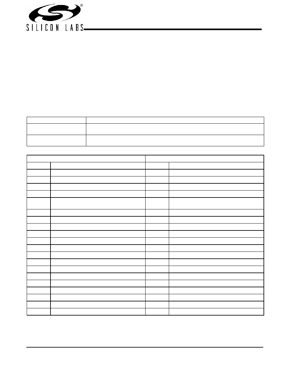
Table 3. Command Code Definition
Bit
Descriptions
7
0 = Block read or block write operation
1 = Byte read or byte write operation
6:0
Byte offset for byte read or byte write operation. For block read or block write operations, these
bits should be ‘0000000’.
Table 4. Block Read and Block Write Protocol
Block Write Protocol
Block Read Protocol
Bit
Description
Bit
Description
1
Start
1
Start
2:8
Slave address – 7 bits
2:8
Slave address – 7 bits
9
Write = 0
9
Write = 0
10
Acknowledge from slave
10
Acknowledge from slave
11:18
Command Code – 8 Bit
'00000000' stands for block operation
11:18
Command Code – 8 Bit
'00000000' stands for block operation
19
Acknowledge from slave
19
Acknowledge from slave
20:27
Byte Count – 8 bits
20
Repeat start
28
Acknowledge from slave
21:27
Slave address – 7 bits
29:36
Data byte 1 – 8 bits
28
Read = 1
37
Acknowledge from slave
29
Acknowledge from slave
38:45
Data byte 2 – 8 bits
30:37
Byte count from slave – 8 bits
46
Acknowledge from slave
38
Acknowledge
....
......................
39:46
Data byte from slave – 8 bits
....
Data Byte (N–1) –8 bits
47
Acknowledge
....
Acknowledge from slave
48:55
Data byte from slave – 8 bits
....
Data Byte N –8 bits
56
Acknowledge
....
Acknowledge from slave
....
Data bytes from slave/Acknowledge
....
Stop
....
Data byte N from slave – 8 bits
....
Not Acknowledge
....
Stop
发布紧急采购,3分钟左右您将得到回复。
相关PDF资料
CY284108ZXC
IC CLOCK SERV CK410B 56TSSOP
CY28410OXC-2
IC CLOCK CK410 GRANTSDALE 56SSOP
CY28410OXC
IC CLOCK CK410 GRANTSDALE 56SSOP
CY28411ZXC
IC CLOCK CK410M ALVISO 56TSSOP
CY28442ZXC-2
IC CLOCK ALVISO PENTM 56TSSOP
CY28445LFXC-5
IC CLOCK CALISTOGA CK410M 68QFN
CY28446LFXC
IC CLOCK CALISTOGA CK410M 64QFN
CY28447LFXC
IC CLOCK CALISTOGA CK410M 72QFN
相关代理商/技术参数
CY28378OXCT
功能描述:时钟发生器及支持产品 Sys Clk Pentium 4 & Intel Brookdale 845 RoHS:否 制造商:Silicon Labs 类型:Clock Generators 最大输入频率:14.318 MHz 最大输出频率:166 MHz 输出端数量:16 占空比 - 最大:55 % 工作电源电压:3.3 V 工作电源电流:1 mA 最大工作温度:+ 85 C 安装风格:SMD/SMT 封装 / 箱体:QFN-56
CY28381
制造商:CYPRESS 制造商全称:Cypress Semiconductor 功能描述:High-Performance SiS645DX/648DX/650/651 Intel Pentium 4 Clock Synthesizer
CY28381OC
制造商:Rochester Electronics LLC 功能描述:- Bulk 制造商:Cypress Semiconductor 功能描述:
CY28381OCT
制造商:CYPRESS 制造商全称:Cypress Semiconductor 功能描述:High-Performance SiS645DX/648DX/650/651 Intel Pentium 4 Clock Synthesizer
CY28400
制造商:CYPRESS 制造商全称:Cypress Semiconductor 功能描述:100-MHz Differential Buffer for PCI Express and SATA
CY28400_05
制造商:CYPRESS 制造商全称:Cypress Semiconductor 功能描述:100-MHz Differential Buffer for PCI Express and SATA
CY28400-2
制造商:CYPRESS 制造商全称:Cypress Semiconductor 功能描述:100-MHz Differential Buffer for PCI Express and SATA
CY28400OC
功能描述:时钟缓冲器 100 MHz Diff Buffer PCI Express & SATA RoHS:否 制造商:Texas Instruments 输出端数量:5 最大输入频率:40 MHz 传播延迟(最大值): 电源电压-最大:3.45 V 电源电压-最小:2.375 V 最大功率耗散: 最大工作温度:+ 85 C 最小工作温度:- 40 C 封装 / 箱体:LLP-24 封装:Reel